
Smectic Films and Focal Conic Domains

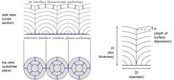
Fig. 1: Left: schematic cross section through a row of focal conic domains and top view on the substrate plane; the blue ellipses symbolize the liquid-crystal molecules and the curved black lines the smectic layer planes. Right: dimensions of a single focal conic domain; diameter2r and film thickness H are typically between some μm and a few tens of μm, the depth h of the depressions in the air interface can amount up to one or two μm.
 adopt for toroidal FCDs the shape of a circle and a straight line (in general, they form an ellipse and a hyperbola intersecting each others focal point).")
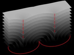
Fig. 2: Cross section through two toroidal focal conic domains. The two singular lines (drawn in red) adopt for toroidal FCDs the shape of a circle and a straight line (in general, they form an ellipse and a hyperbola intersecting each others focal point).

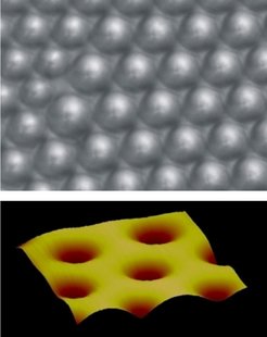
Fig. 3: Top: Optical micrograph of a lattice of FCDs in a smectic film on a silicon wafer inducing randam planar anchoring of the liquid crystal. Bottom: AFM image obtained for the same sample, the depth of the defect-induced depressions amounts to 250 nm, the lateral dimension of the shown area is 25 μm.
 is confined to these lines.")
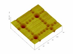
Fig. 4: AFM image of a smectic film on a patterned substrate. Random planar anchoring is induced on 15 μm wide lines of a square-like grid pattern. The generation of focal conic domains (indicated by the surface depressions) is confined to these lines.
![Fig. 5: Relation between the diameter 2r of the FCDs and the thickness H of the smectic film. The two data sets are obtained for two substrates possessing different strengths of the random planar anchoring. The anchoring strength was tuned by coating the silicon wafers with differently composed silane mixtures. Solid lines are fits to a theoretical model [J. B. Fournier, I. Dozov, G. Durand, Phys. Rev. A 41, 2252 (1990)].](/3205620/original-1518437630.webp?t=eyJ3aWR0aCI6MTY5NiwiZmlsZV9leHRlbnNpb24iOiJ3ZWJwIiwib2JqX2lkIjozMjA1NjIwfQ%3D%3D--cc20e8b830c72f58fc8385acd6eb40847a5d8c78 "Fig. 5: Relation between the diameter 2r of the FCDs and the thickness H of the smectic film. The two data sets are obtained for two substrates possessing different strengths of the random planar anchoring. The anchoring strength was tuned by coating the silicon wafers with differently composed silane mixtures. Solid lines are fits to a theoretical model [J. B. Fournier, I. Dozov, G. Durand, Phys. Rev. A 41, 2252 (1990)].")
![Fig. 5: Relation between the diameter 2r of the FCDs and the thickness H of the smectic film. The two data sets are obtained for two substrates possessing different strengths of the random planar anchoring. The anchoring strength was tuned by coating the silicon wafers with differently composed silane mixtures. Solid lines are fits to a theoretical model [J. B. Fournier, I. Dozov, G. Durand, Phys. Rev. A 41, 2252 (1990)].](/3205620/original-1518437630.jpg?t=eyJ3aWR0aCI6MjQ2LCJvYmpfaWQiOjMyMDU2MjB9--4ff29d80ff4ccbeeaa55305f270e741613786ffb)
Fig. 5: Relation between the diameter 2r of the FCDs and the thickness H of the smectic film. The two data sets are obtained for two substrates possessing different strengths of the random planar anchoring. The anchoring strength was tuned by coating the silicon wafers with differently composed silane mixtures. Solid lines are fits to a theoretical model [J. B. Fournier, I. Dozov, G. Durand, Phys. Rev. A 41, 2252 (1990)].
 in 40 μm thick films of various liquid crystal compounds. The four upper data sets belong to compounds possessing a smectic-A–isotropic transition, the two lower data sets belong to compounds possessing a smectic-A–nematic transition.TA↔N/I designates the smectic-A–nematic or smectic-A–isotropic transition temperature (solid lines are just guides to the eyes).")

Fig. 6: Left: Relation between film thickness H, FCD diameter 2r, and depth h0 of the surface depression for strictly incompressible layers. Right: Temperature dependence of the ratio h/h0 (h: measured depth of the FCD-induced surface depressions, h0: calculated values assuming incompressible layers) in 40 μm thick films of various liquid crystal compounds. The four upper data sets belong to compounds possessing a smectic-A–isotropic transition, the two lower data sets belong to compounds possessing a smectic-A–nematic transition.TA↔N/I designates the smectic-A–nematic or smectic-A–isotropic transition temperature (solid lines are just guides to the eyes).


Fig. 7: Smectic-A film on a unidirectional planar anchoring substrate. A linear structure with smooth surface corrugations is formed.
 smectic-A film on a unidirectional planar substrate. The smooth surface corrugations of Fig. 7 become decorated with additional features.")

Fig. 8: Thicker (≈ 10 μm) smectic-A film on a unidirectional planar substrate. The smooth surface corrugations of Fig. 7 become decorated with additional features.

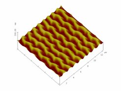
Fig. 9: Smectic-C film on a unidirectional planar substrate.